Tel: +86-371-65960666 Mobile: +86-13837180668 E-mail: wmsale@hxkjgf.com


Polycrystalline Solar Wafer
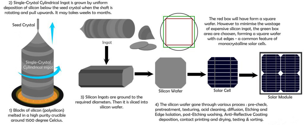
Introduction of silicon wafer
Hengxing is the main manufacturer for silicon wafers PV module. Our Polycrystalline Solar Wafer can be manufactured to the exact requirements of producers, with customized choices on hand for thickness, geometry, bevel facet and more.
Polycrystalline silicon wafer is the core material of solar cell, which is widely used in the fields of photovoltaic power generation, communication, traffic and the production and living power supply of residents in remote areas.
Performance parameter
Dimension:156×156±0.5mm
Thickness:200±20um/240±20um
Diameter:219.2±0.5mm
Conductivity:P Type(Boron Doped)
Resistivity:0.5~2Ω·cm
Minority Carrier Lifetime:≥2us
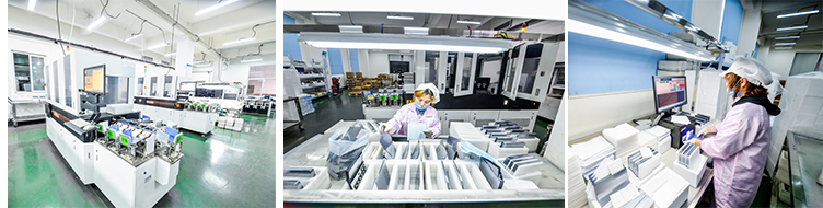
Testing equipment for silicon wafer
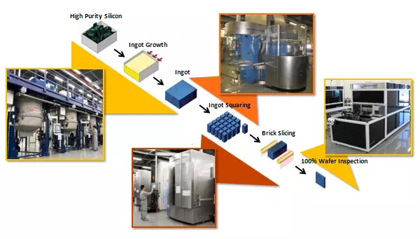
Factory production flow chart
Our service
1. Our sales representative and engineer work together to answer your questions and offer a solution for free.
2. We choose the best product for you to make sure it worth its real value
3. We design the best solution with good performance for you, meanwhile, save every cent of your money.
Frequently asked questions (FAQ)
Q: Do you provide samples?
A: We can provide you with samples and we invite you to visit our factory at any time.
Q: Can I customize the products according to my needs?
A: Yes, we can customize the material, specifications and optical coating for your optical components according to your needs.
Q: Do you have an inspection report for the material?
A: We can supply ISO, CE, etc. For our products.
Physical Characteristics of silicon wafer
|
Item |
Polycrystalline silicon wafer |
|
Technology |
Diamond wire cutting |
|
Type |
P type |
|
Resistance |
1~3Ωcm |
|
minority carrier |
>2μs |
|
Hem width |
156.75~157.25mm |
|
Thickness |
200±20μm |
|
The angle of Chamfer |
1~2mm |
|
Transfer efficiency |
>18.8% |
|
shape |
square |
|
Place of Origin |
Henan, China(Mainland) |
|
Brand Name |
High-efficiency polysilicon sheet |
Copyright © Henan Hengxing Technology Co., Ltd. Powered by www.300.cn 豫ICP备97845788号

Contact Us
Tel:
+86-371-67635666
+86-13837180668
+86-371-66908222
wmsale@hxkjgf.com
Fax:
E-mail:
Products
Messages